- 您现在的位置:买卖IC网 > Sheet目录320 > DK-DEV-4SE530N (Altera)KIT DEV STRATIX IV FPGA 4SE530
�� �
�
�A.� Programming� the� Flash� Memory�
�Device�
�As� you� develop� your� own� project� using� the� Altera� tools,� you� can� program� the� flash�
�memory� device� so� that� your� own� design� loads� from� flash� memory� into� the� FPGA� on�
�power� up.� This� appendix� describes� the� preprogrammed� contents� of� the� common� flash�
�interface� (CFI)� flash� memory� device� on� the� Stratix� IV� E� FPGA� development� board� and�
�the� Nios� II� EDS� tools� involved� with� reprogramming� the� user� portions� of� the� flash�
�memory� device.�
�The� Stratix� IV� E� FPGA� development� board� ships� with� the� CFI� flash� device�
�preprogrammed� with� a� default� factory� FPGA� configuration� for� running� the� Board�
�Update� Portal� design� example� and� a� default� user� configuration� for� running� the� Board�
�Test� System� demonstration.� There� are� several� other� factory� software� files� written� to�
�the� CFI� flash� device� to� support� the� Board� Update� Portal.� These� software� files� were�
�created� using� the� Nios� II� EDS,� just� as� the� hardware� design� was� created� using� the�
�Quartus� II� software.�
��page� of� the� Altera� website.�
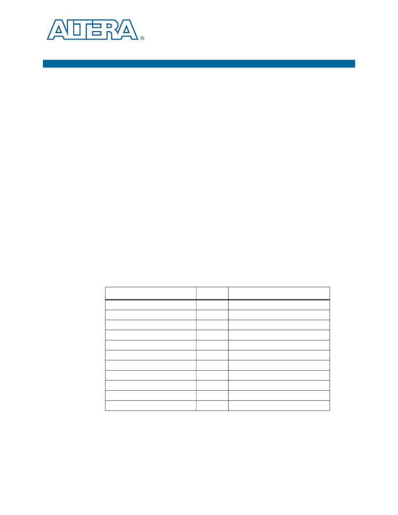
�CFI� Flash� Memory� Map�
��device.� For� the� Board� Update� Portal� to� run� correctly� and� update� designs� in� the� user�
�memory,� this� memory� map� must� not� be� altered.�
�Table� A–1.� Byte� Address� Flash� Memory� Map�
�Block� Description�
�Unused�
�User� software�
�User� hardware�
�Reserved�
�zipfs� (html,� web� content)�
�Factory� software�
�Factory� hardware�
�PFL� option� bits�
�Board� information�
�Ethernet� option� bits�
�User� design� reset� vector�
�Size� (KB)�
�128�
�11,699�
�21,627�
�128�
�5,898�
�5,898�
�21,627�
�32�
�32�
�32�
�32�
�Address� Range�
�0x03FE.0000� -� 0x03FF.FFFF�
�0x034C.0000� -� 0x03FD.FFFF�
�0x0202.0000� -� 0x034B.FFFF�
�0x0200.0000� -� 0x0201.FFFF�
�0x01A6.0000� -� 0x01FF.FFFF�
�0x014C.0000� -� 0x01A5.FFFF�
�0x0002.0000� -� 0x014B.FFFF�
�0x0001.8000� -� 0x0001.FFFF�
�0x0001.0000� -� 0x0001.7FFF�
�0x0000.8000� -� 0x0000.FFFF�
�0x0000.0000� -� 0x0000.7FFF�
�c� Altera� recommends� that� you� do� not� overwrite� the� factory� hardware� and� factory�
�software� images� unless� you� are� an� expert� with� the� Altera� tools.� If� you� unintentionally�
�overwrite� the� factory� hardware� or� factory� software� image,� refer� to� “Restoring� the�
��June� 2011�
�Altera� Corporation�
�Stratix� IV� E� FPGA� Development� Kit� User� Guide�
�发布紧急采购,3分钟左右您将得到回复。
相关PDF资料
DK-DEV-4SGX530N
KIT DEVELOPMENT STRATIX IV
DK-DEV-5AGXB3N/ES
ARRIA V DEVELOPMENT KIT
DK-DEV-5M570ZN
KIT DEV MAX V 5M570Z
DK-DEV-5SGXEA7N
KIT DEV STRATIX V FPGA 5SGXEA7
DK-DSP-2S180N
DSP PRO KIT W/SII EP2S180N
DK-DSP-3C120N
KIT DEV DSP CYCLONE III EDITION
DK-K7-CONN-CES-G
KINTEX-7 FPGA CONNECTIVITY KIT
DK-K7-EMBD-CES-G-J
KINTEX-7 FPGA EMBEDDED KIT JAPAN
相关代理商/技术参数
DK-DEV-4SGX230N
功能描述:可编程逻辑 IC 开发工具 FPGA Development Kit For EP4SGX230KF40C2N
RoHS:否 制造商:Altera Corporation 产品:Development Kits 类型:FPGA 工具用于评估:5CEFA7F3 接口类型: 工作电源电压:
DK-DEV-4SGX230N/C2
功能描述:EP4SGX230KF40C2N Stratix? IV GX FPGA Evaluation Board 制造商:altera 系列:Stratix? IV GX 零件状态:过期 类型:FPGA 配套使用产品/相关产品:EP4SGX230KF40C2N 内容:板,线缆,电源 标准包装:1
DK-DEV-4SGX530N
功能描述:可编程逻辑 IC 开发工具 FPGA Development Kit For EP4SGX530
RoHS:否 制造商:Altera Corporation 产品:Development Kits 类型:FPGA 工具用于评估:5CEFA7F3 接口类型: 工作电源电压:
DK-DEV-5AGTD7N
功能描述:可编程逻辑 IC 开发工具 FPGA Development Kit For 5AGTD7K3F40I3N
RoHS:否 制造商:Altera Corporation 产品:Development Kits 类型:FPGA 工具用于评估:5CEFA7F3 接口类型: 工作电源电压:
DK-DEV-5AGXB3N/ES
功能描述:可编程逻辑 IC 开发工具 FPGA Development Kit For 5AGXFB3H6F ES RoHS:否 制造商:Altera Corporation 产品:Development Kits 类型:FPGA 工具用于评估:5CEFA7F3 接口类型: 工作电源电压:
DK-DEV-5ASTD5N
功能描述:KIT DEV ARRIA V FPGA 制造商:altera 系列:Arria V ST 零件状态:在售 类型:FPGA 配套使用产品/相关产品:Arria? V ST 内容:板 标准包装:1
DK-DEV-5CEA7N
功能描述:可编程逻辑 IC 开发工具 FPGA Development Kit For 5CEFA7F31C7N
RoHS:否 制造商:Altera Corporation 产品:Development Kits 类型:FPGA 工具用于评估:5CEFA7F3 接口类型: 工作电源电压:
DK-DEV-5CEA7N/P
制造商:Altera Corporation 功能描述:Cyclone VE Devkit Promotional 制造商:Altera 功能描述:Cyclone VE Devkit Promotional